In digital electronics any signal can hold four values that are
- 0 - LOW
- 1 - HIGH
- x - Unknown - Either 0 or 1.
- z - High Impedance
Consider a case where we have D flip-flop and there is change in data signal (D) at positive edge of the clock (clk). As shown in shaded reason in timing diagram.
Here we can not predict the output (Q) because 'D' is unstable at positive edge of 'clk'. So it is Neither 0 nor 1. This state is called metastable state. Generally it accrues when there are setup and hold violations in design. We should take care of it in advance otherwise it can make whole system metastable.
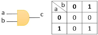
There is one more condition which can make system unstable that is due to combinational logic change. Let us take an example of 2 input AND gate. Truth table of 2 input AND gate is
 |
| AND Gate and Truth Table |
From the above truth table the output of AND gate is ‘zero’ for input ‘01’ and ‘10’. When input change from ‘01’ to ‘10’, it can take following two path
- 01 -> 00 -> 10
- 01 -> 11 -> 10
When it takes 1st path then output remains ‘0’, but when it take 2nd path then output goes from 0 to 1 then 0. This HIGH output accrue for very short duration. This is called Glitch and this may cause metastability in system. Similar behavior for OR gate also there is LOW output accrue for very short duration.
 |
| OR Gate and Transitions between 01 to 10 and via-versa |
Sometime we can see this behavior in netlist simulation. Designers use Gray Code Technique where small glitch can affect the design. In Gray code only one bit change at a time.
More Useful Links...
- Basics of Setup and Hold
- Basics of Jitter and Skew
- Metastable State


No comments:
Post a Comment