- What is FPGA ?
ANS : FPGA - Field Programmable Gate Array.
It is a device with programmable ‘logic blocks’ and programmable ‘interconnects’. Logic blocks contain LUTs and CLBs which used to implement mathematical or logical functions and interconnect join them to make large design. It uses external memory to store the interconnection information. This information can be changed and device can be reprogrammed by prototype designer.
- Draw the general structure of FPGA ?
ANS : FPGA - Basically it consists of programmable ‘Logic Blocks’ and ‘Interconnects’.
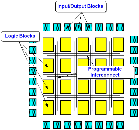
Logic Blocks contains CLB (Configurable Logic Block) and each CLB contain some LUTs (Look-Up-Table) and other logic.
- Explain CLB’s and LUT’s of FPGA ?
ANS : Logic Blocks primarily contain programmable CLBs and LUTs.
- CLB (Configurable Logic Block) - These are the main logic resource for implementing sequential as well as combinatorial circuits. A CLB elements contains a pair of ‘slices’. They don’t have direct connection to each other. Each slice has contain independent carry chain.
- LUT (Look Up Table) - Each Slice contains four or six input look-up-table (LUT), storage elements, multiplexers and carry logic. These element are used to provide logic, arithmetic and ROM functions. Some slice contains additional functions like Distributed RAM and shifting data 32-bit.
- Steps for FPGA Prototyping ?
ANS : Find the FPGA prototyping design flow in following link.
- What are the differences between FPGA and ASIC also give pros and cons ?
ANS : FPGAs (Field Programmable Gate Arrays) and ASICs (Application Specific Integrated Circuits) both have their advantages. FPGA’s are reprogrammable but costly where ASIC’s are non-programmable and application specific but cheap. Let’s look
FPGA Advantages
1.
|
Field Reprogrammable
|
Bitstream can be uploaded remotely.
|
2.
|
Simple design cycle
|
Tool take care of routing, placement and timing.
|
3.
|
Faster time to market
|
No layout, masking or fabrication needed.
|
ASIC Advantages
1.
|
Full custom capability
|
Device is manufactured with design specs.
|
2.
|
Lower unit cost
|
Generally cost is lower due to mass production.
|
- What is Synthesis ?
ANS : Synthesis is the process of translating HDL code into gates. Synthesis tools take HDL code and gives gate level netlist output for selected device. Please go through following link for more information-
- List of synthesizable and non-synthesizable constructs ?
ANS : Please go through following link for synthesizable and non-synthesizable constructs information-
- What is DRC and difference between DRC and LVS ?
ANS : DRC : Design Rule Check
In ASIC there are some sets of rules which depends on technology used to design. Means some sets of parameters which decide where the mask should be placed, connected and routed in the layout. This check has responsibility of design to work after fab process.
In FPGA, tool (like vivado) check the correctness of the design before synthesis, which is also said DRC check.
LVS : Layout Versus Schematic
DRC ensure that layout conforms the rule required for faultless fabrication. But it is not guaranteed layout contain same circuit you desire to fab. Here the LVS check required. This process matches the netlist extracted from layout versus the original schematic or circuit.
- What is stuck at ZERO Means ?
ANS : Some time in ASIC due to some fault any node will permanent tie to either ‘0’. This is called Stuck at ZERO error. Similarly stuck at ONE error. To check this error we need to provide some testability in RTL.
It generally not appears in FPGA prototyping, these are tested hardware which are programmed by bit file not fabricated so probability of error is less.
- What is DFT and do it require in FPGA prototyping ?
ANS : DFT : Design for Testability.
Check the toggling of each flop in the design and eliminate the manufacturing error like stuck at ‘0’ or ‘1’, DFT process is used. Apart from the functional logic DFT logic are also added in design and patterns are generated so that we can test the manufacturing defects after it come from fab. Scan chain, MBIST and LBIST are the part of this test.
- What are MBIST and LBIST in DFT ?
ANS : BIST : Built in Self Test.
Two most common method for DFT testing are Logic BIST (LBIST) and Memory BIST (MBIST).
LBIST is design for testing random logic, which use pseudo random pattern generator (PRPG) to generate input pattern and multiple input signature register (MISR) for obtaining the response of the device for there input pattern. An incorrect MISR output indicate the defect in the device.
MBIST is design for testing memory, which use various algorithm to test memory by writing, reading and comparing. MBIST check following faults in memories
- Stuck-at Fault
- Transition Fault
- Coupling Fault
- Neighborhood Pattern Sensitive Fault
- Address Decoding Fault.
“March” Algorithm is most common algorithm used in industry.
- What are the differences between FPGA and CPLD ?
ANS : FPGA : Field Programmable Gate Array.
CPLD : Complex Programmable Logic Device.
Function of both the devices are same but difference in
- Capacity : Normally CPLD has less capacity than FPGA.
- Image Storage : CPLD can bootup by itself but FPGA has large boot image and it fetches image from SRAM.
- Features : CPLD only provide gates but FPGA also provides hard blocks like Block RAM, DSP, Microprocessor etc. which make FPGA more suitable for embedded systems.
- What is DCM, Why the are used ?
ANS : DCM : Digital Clock Manager
DCM is an electronic component which uses the feedback path to maintain the clock signal despite normal variation in operating temperature and voltage. The output of DCM gives clock with minimum skew with high fanout, because it uses global buffer for high fanout.
- What are differences between DLL and PLL ?
ANS : DLL : Delay Lock Loop
PLL : Phase Lock Loop
These are two technique to minimize the clock skew.
- PLL use voltage-controlled-oscillator (VCO) whereas DLL use delay line.
- PLLs are hybrid analog and digital whereas DLLs are all digital.
- DLL have step errors but hybrid PLL does not have it.
- DLL have less clock skew than PLL.
- What are the different modes of programming the FPGA ?
ANS : There are many modes of programming the FPGA.
- SRAM via JTAG or programmable cable.
- Flash.
- USB and SD-Card.
- What is constraint file and why we use it ?
ANS : Constraint file required for make design as per your requirements, like there is need to take out some signals to particular pins of FPGA eg. JTAG or define clocks as false path or multi-cycle path. More can find from -
- Name the FPGA manufacture companies ?
ANS : FPGA Companies
- Xilinx (~50%)
- Altera (~40%)
- Lattice Semiconductor
- Microsemi (Actel)
- QuickLogic
- What is the difference between ‘Hard Processor Core’ and ‘Soft Processor Core’ ?
ANS : Generally FPGA are categorized in following two ways in terms of design.
- Hard Processor Core - Some part of FPGA has fixed blocks like processor core and some common standard IPs. Little space for other logic implementation.
- Capable of work on high speed due to better optimization.
- But have fixed configuration and can not be altered.
- Soft Processor Core - Full FPGA can be used for logic. User need to implement soft processor core if required.
- Can be easily modified and have more logic.
- But limited in terms of speed of the fabric.
- How you can know the maximum allowable operating frequency of your design ?
ANS : Maximum allowable frequency is limit by ‘Setup Violation’ in FPGA design. Timing report generated for the given clock frequency. If minimum ‘Slack’ between two flops is positive then we can decrease the time period by that amount or increase the frequency.
- How you can increase the operating frequency of the design in FPGA ?
ANS : There are following ways which might use to increase the operating frequency of the design
- Check timing critical path and optimized it.
- Proper design constraint and timing constraint.
- Pipeline structure.
- What is minimum and maximum frequency of DCM in Spartan-3 and Virtex-5 series FPGA ?
ANS : Minimum and maximum frequency of DCM in
- Spartan-3 : 24 MHz to 248 MHz
- Virtex-5 : up to 550 Mhz
- Can CLB configured as a RAM ?
ANS : In Xilinx CLB has two slices which is Slice-L and Slice-M. Function generators (LUTs) in Slice-M can be implemented as a synchronous RAM called distributed RAM. Multiple LUTs in Slice-M can be combined in various ways to store large amount of data.
- What is Global Buffers, give some example ?
ANS : Global Buffer - Distribute the high fanout signals throughput.
In Xilinx FPGA there are many types of global buffers available like BUFG, BUFGMUX, BUFGCE etc. Different FPGA has limited global buffers and apart from tool user can explicitly use them also by using constraint file.
- Is there is any way to use the design in FPGA which has ‘setup violation’ ?
ANS : Setup violation accrue if net delay between flops are greater than Time period of the clock. So if we can increase the time period of clock such that it is greater than or equal to net delay then we can use that same FPGA design. Increase the time period means decrease in frequency so by lowering the clock frequency can make design work.
- Is there is any way to use the design in FPGA which has ‘hold violation’ ?
ANS : Hold violation accrue when path delay is less than the hold time of the flop. So by adding some path delay we can use the design. But that path delay should not exceed the time period of clock.
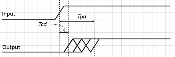
- What is ‘contamination delay’ in sequential circuit and difference with propagation delay ?
ANS : Contamination Delay (Tcd) : Minimum time that the logic gate will change the output based on change in input.
Propagation Delay (Tpd) : Maximum time that the logic gate will change the output based on change in input.
- Which are the different reports we need to look while FPGA prototyping ?
ANS : At different phase of FPGA prototyping following report are generated
- Synthesis report after synthesis.
- Place & Route and
- Timing report after Place and route or bit file generation.
- Which primary information are need to look in above reports ?
ANS : Following main information need to look in synthesis report
- Signals or registers which are optimized or prune.
- Latches in the design.
Following information need to look in P&R and timing report
- Setup and Hold Violation.
- Are the clock constraints applied properly.
- False path and multi cycle path.
- Gate count.
- What are different type of RAMs in FPGA and how we can use them ?
ANS : Xilinx FPGA provides two options for creating memories for storing data.
- Distributed Memory : Array of register.
- Block Memory : Dedicated memory.
When synthesis tool synthesize the RTL then it can use any memory depends on your coding. Before move on to coding style first see the difference between them.
- When it require to make small data memory, like small buffers or registers then use distributed memory.
- When it require to store large amount of data, like data message buffers or large lookup table then use block memory. This memory is limited and depends on FPGA series.
We should not use distributed memory for storing large amount of data because it use large number of logic cells/flops to make register and will take large number of registers to make memory.
//Let’s see the verilog code for configure block RAM
module B_RAM (clk, addr, we, data_in, data_out);
input clk, we ;
input [1:0] addr ;
input [15:0] data_in ;
output [15:0] data_out ;
reg [15:0] mem [3:0] ;
reg [15:0] data_r ;
assign data_out = data_r ;
always @ (posedge clk) begin
if (we) begin
mem [addr] <= data_in ;
end
data_r <= mem [addr] ;
end
endmodule
NOTE : Initialization the RAM separately.
- What is the difference between ‘reg’ and ‘wire’ ?
ANS : In HDL language ‘wire’ is which connects two nodes, it can not store data and used for designing combinational logic.
Whereas ‘reg’ can store the value and drive strength. It can use for modeling both combinational and sequential logic. Reg data type can be initial and always block.
- What is different type of ‘timing verification’ ?
ANS : There are two type timing verification -
- Dynamic timing
- Static Timing
- What does ‘timescale 1ns/1ps’ signifies ?
ANS : Timescale specify the time unit and precision of a module. It is written as
timescale time_unit_base / precision_base
From above example ‘timescale 1ns/1ps’, the base of time unit is in nanosecond and base of precision is in picosecond. Time unit is amount of time a delay #1 represents and precision is how many decimal points of precision to use relative to the time unit.
- Different Debug tools used in FPGA design debugging ?
ANS : Each FPGA Tool manufacturing company will also make some tools for debugging like
- Chipscope - Xilinx
- Protolink - Synopsis
- On-Chip Debugging - Altera
- What is ‘Emulation’ and difference from ‘FPGA platform’ ?
ANS : Emulation word sound similar to simulation and work similar to that also. In simulation compiler break the code into nodes and calculate the value of each node at each clock edge. Emulation platform is actually group of processors which make can separate thread for each node. It work on synthesized design. Emulation platform is a hardware so we can connect debugger and other peripherals with it.
It is similar to FPGA but have following differences
- Capacity : Emulation Platform has very large capacity compare to FPGA. You can emulate full Soc in emulation platform.
- Speed : Emulation platform work on KHz to few MHz whereas FPGA work on 10 to 100 MHz. So FPGA are 100 times faster than Emulation.
- Debug : Emulation platform gives facility to take waveform dump at anytime at any trigger condition, but FPGA you need to add extra logic plus select the signal previously which we want to check.
- Force : In emulation we can force any value to any signal but in FPGA we can not do this.
- Timing : In FPGA we need to do Place and Route after synthesis but in Emulation platform we need not to do P&R.
- What is the difference between ‘rtl simulation’ and ‘netlist simulation’ ?
ANS : In simulation compiler do and don’t do the following operation
- Do the syntax check
- Don’t optimize the code
- Don’t synthesize the code means non-synthesizable construct can be use in simulation, eg. delay, initial, fork join etc.
- Do break the code into nodes and calculate the value of each node for each clock edge. So as your design increases, number of nodes increases and hance take more time to run complete simulation. Also it dumps the waveform for each clock edge.
- Don’t change the signal name.
In RTL simulation, tool compile the code and determine the nodes and dump the value of each nodes at each clock cycle. Whereas netlist generate after the synthesis in which RTL code is optimized and change into gate level. This increase the number of nodes and take more time in simulation compared to RTL simulation.
36. Which one of following is not synthesizable VHDL statement ?
- ‘case’
- ‘wait until’
- ‘wait for’
- ‘generate’
ANS : ”wait for” is non synthesizable.
Under process ‘wait until’ is synthesizable.
No comments:
Post a Comment