Showing posts with label setup. Show all posts

Wednesday, March 9, 2016

Basics of Setup and Hold Part -2

Clock plays very crucial role in sequential circuits but Skew and Jitter in clocks can make the stable circuit to unstable. Let’s discuss this one by one what are skew and jitter also how they affect the sequential circuit.

CLOCK SKEW
In circuit designs, clock skew is a phenomenon in synchronous circuits in which the same sourced clock signal arrives at different components (generally latches or flip-flops) at different times. This is due to interconnects delay and clock buffer delay.
clock_skew
Clock Skew
Suppose when there is no clock buffers then clock edge reaches at launch flop at time t=0 and due to clock buffer 1 and 2 in the path of launch flop it reaches at time t = D1 + D2.
Similar for capture flop when there is no clock buffers then clock edge reaches at time t = T but due to clock buffers delay in clock path it reaches at time 
t = T + D1 + D3 + D4.
If we assume clock edge reaches in launch flop at time t = T1 and next edge reaches at capture flop at time t = T2 then we can say
CLOCK SKEW = |T2 - T1 - T|
Or
CLOCK SKEW = |(D1+D3+D4) - (D1+D2)|

CLOCK JITTER
Deviation or displacement of a periodic signal from its true position is called jitter. Electromagnetic interference and crosstalk are major cause for jitter in clock.
clock_jitter
Clock Jitter
While calculation of setup delay we subtract jitter time or uncertainty (U) from clock period (T). So actual time period is now T - U.

THE EFFECT OF 'SKEW' AND 'JITTER' IN SETUP & HOLD TIME ANALYSIS
Now let us look the effect of ‘clock skew’ and ‘clock jitter’ in setup and hold time analysis of two flop network. Setup delay equation from previous blog
Tc2q + Tpd  <  T - Ts
When there is jitter in clock then the setup time equation become
Tc2q + Tpd  <  T - Ts - U
Also consider the clock delay in network then it become
Tc2q + Tpd + (D1 + D2) <  (T + D1 + D3 + D4) - Ts - U
This can be understand by following timing diagram.


effect_of_jitter_and_skew_in_setup_analysis
Effect of Jitter and Skew in Setup Analysis

Hold delay is not much affected by clock jitter and skew because we analyze it at same clock edge. We can understand it by following timing diagram.

effect_of_jitter_and_skew_on_hold_analysis_d4s
Effect of Jitter and Skew on Hold Analysis

In NEXT blog there are some exercise questions asked in interviews and competitive exams. This also help in to better understanding of the concept of setup and hold time. Hope you enjoy them also.

Saturday, February 13, 2016

Basic of Setup and Hold

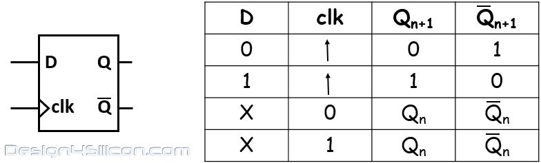
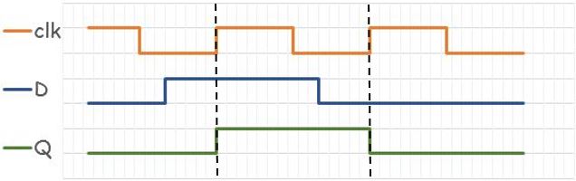
We all know about D or Delay Flip-Flops. It is edge triggered device which transfer input (D) to output (Q) on its rising or falling of clock (clk). Truth table and timing diagram of D Flip-flop is

DFF_with_Truth Table.JPG
D Flip Flop and Truth Table
DFF_with_timing_diagram_1.JPG
D-Flip Flop Timing Diagram
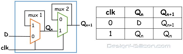
Above simulation timing diagram do not include the delay of D flip-flop. We can analyze this delay's behavior of D flip-flop by following two mux diagram.
DFF_with_2_mux.JPG
Two MUX diagram of D Flip Flop with Truth Table
Let’s take delays of mux-1 and mux-2 are t1 and t2 respectively. When clk is ‘0’ then mux-1 take at least t1 time to update the value from 'D' to 'Qn' and when clk is ‘1’ then 'Qn' is remains same. During t1 time input 'D' must not change. This t1 time is called Setup Time (Ts). So the setup time is the time interval before clock where input ‘D’ must held stable.

Similarly for mux-2 when clk is ‘1’ then mux-2 takes at least t2 to update the value from 'Qn' to 'Qn+1' and when clk is ‘0’ then 'Qn+1' is remains same. During t2 time input 'Qn' must not change. This t2 time is called Hold Time (Th). So the hold time is the time interval after clock where input ‘Qn’ must held stable.

There is one more timing property which we should also need to understand with setup and hold i.e. 'clock to Q' delay. Time interval from clock input to data out from flop.
Timing Diagram of two mux D flip-flop


Summery : Important timing parameter of Flip-Flop are.
Setup Time (Ts) : Till the time input ‘D’ remains stable before the clock edge.
Hold Time (Th) : Till the time input ‘D’ remains stable after the clock edge.
Clock to Output Time (Tc2q) : Time between input clock edge to the output ‘Q’.

SETUP TIME ANALYSIS IN NETWORK For synchronous circuit with in one clock cycle (Tclk) data should transfer from one flop to next flop. This transfer time depends
  1. clock to Q delay of launch flop (Tc2q)
  2. propagation delay of combo logic (Tpd)
  3. setup delay of capture flop (Ts).
setup_time_analysis_d4s
Setup Time Analysis
Let’s introduce the delay in timing equation one by one. From above diagram we can say that for successful transfer of ‘D’ the propagation delay of the combo logic should be less than one clock period.
Tpd < Tclk
Tpdis dynamic delay which depends on combo logic delay and Tc2qand Tsis static delay which are fixed for certain flop. The clock to Q delay of launch flop is the additional delay in path, so combined of Tc2qwith Tpd should be less than one clock period Tclk.
Tpd + Tc2q < Tclk
It is also compulsory that data should arrive at capture flop setup time (Ts) before the clock edge.
Tpd + Tc2q < Tclk - Ts
Till this point we have not include clock uncertainty and clock buffers delay in network. Now from above equation data arrival time is (Tpd + Tc2q) and data required time is (Tclk- Ts).
The difference of data required time to data arrival time is called the SLACK.
SLACK = (Tclk - Ts) - (Tpd + Tc2q)
SLACK can be positive or negative, positive slack means data arrive at capture flop is before the clock edge and negative slack means data arrive at capture flop is after the clock edge also called setup violation.
Setup violation accrue if clock arrives early than data. To avoid setup violation 'maximum data delay' should be smaller than 'minimum clock delay'.

HOLD TIME ANALYSIS IN NETWORK
In a synchronous circuit transfer time should be greater than hold time of the capture flop. Because data should not change too fast so that it violate hold time of capture flop. This transfer time depends on
  1. clock to Q delay of launch flop (Tc2q)
  2. propagation delay of combo logic (Tpd)
hold_time_analysis_d4s
Hold Time Analysis
For proper communication delay should be greater than hold time of capture flop. So
Tc2q+ Tpd > Th
Uncertainty in clock path do not play much role because we use same clock edge for hold time analysis. From above equation data arrival time (Tc2q+ Tpd) should be greater than data require time (Th).
The difference of data arrival time to data required time is called the HOLD SLACK.
SLACK = (Tc2q+ Tpd) - (Th)
SLACK can be positive or negative, positive slack means there is enough delay for capture flop to hold previous data and negative slack means there is less delay and previous data changes before it successfully captured by capture flop this also called hold violation at capture flop.
Hold violation accrue if data arrives early than clock. To avoid hold violation 'maximum clock delay' should be smaller than 'minimum data delay'.

Now also review other timing parameter like clock tree delay and  uncertainty on setup and hold delay in flop network in next part.